TFG part 2 - cgreate

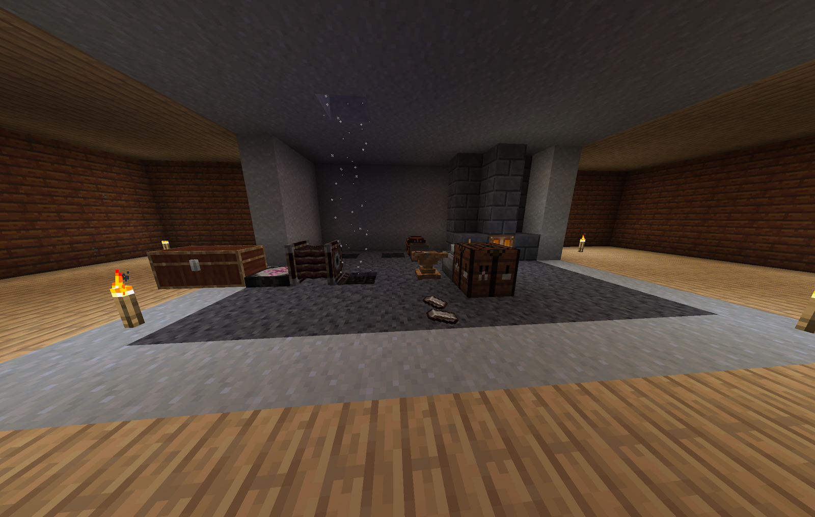
Next on the agenda is create. the todo list is 1) get horse power 2) finish backpack 3) find a real source of EMC in winter 4) figure out how to reach steel? maybe make progress getting there? Our first order of business, however, was getting more food, we ran across half the continent while starving, and managed to find some pumpkins, boars and fish, we also eventually got a harvest of barley and garlic, Some of this even yielded some resources to burn for EMC, mainly bones and some flowers, but our new buffer of 10,000 wouldn't last long and we'll soon need to gather more... We then tamed a horse, and hooked it up to our grinder, threw some hardwood strips into the grinder, some ash into our boiling pot, and built a stomping pot in order to start to create the paper needed for our backpack Waiting 25 minutes for the pulp to dry, until finally we get our backpack, and with it, twice as much inventory space. I'm normally very bad about using things like this, but with the ...