Building SIC-1 in VCB Part 2: DEMUX and Registers
Last part we built the basic components needed, and a RAM prototype, the next step: a demuxer
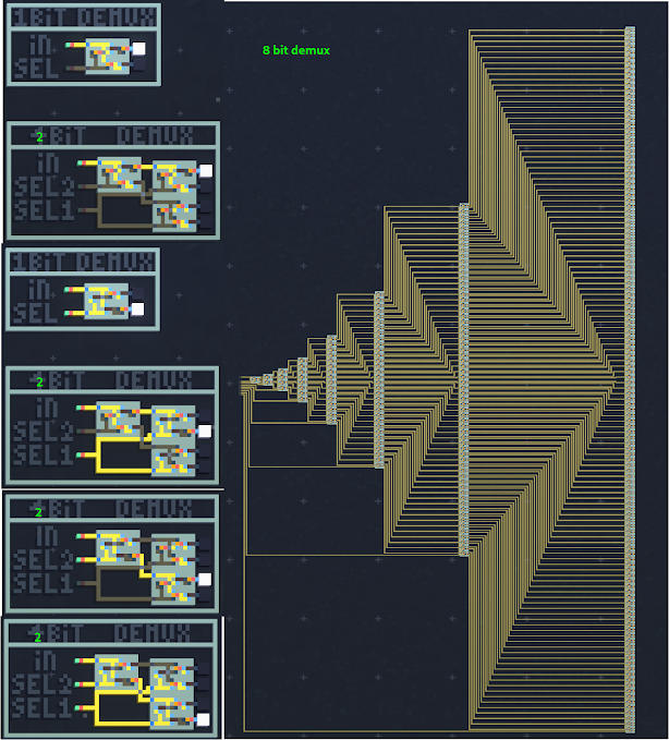
A demuxer is a circuit that can convert an address into a selection, in this case, it's turning a binary address value into a selection from a "bank" of RAM
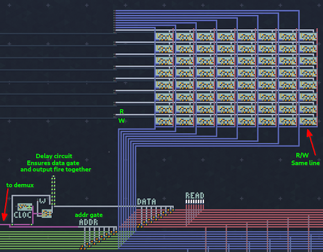
I then refined the RAM prototype to squash it as much as possible, since i was going to have to find a way to squash 256 cells into a workspace that's only about 2048 cells tall, i ended up with this circuit that's just 8 cells tall, though it meant i wouldn't be able to read the data non-destructively, since the circuit reads and writes simultaneously, destroying the old data, but then trying to separate reading and writing would effectively double the amount of wiring as well

Quite some time wiring later, here's the initial design of the full demuxer plus the RAM bank:

Initially i made the "read" bus exit on the bottom, before deciding i'd prefer to have all the inputs in the same place for when the time came to build the actual CPU, so after a bit of wiring and cleanup, because all of this has to be as tiny as possible to stand a chance at fitting the board

The highlighted area in the top is my interface to the rest of the computer, nicely tidying away the nastiness that is this monstrosity, here's a short video showing a few write/read cycles
You'll note the read/write switch, which determines if the output gets sent into the data bus, this is something i initially built out of necessity.
I mentioned earlier on that the RAM blocks read destructively, this means they lose their stored data upon reading, so i made this system to write the data back into the RAM cells as part of the same RAM access, but then i realized it's an "accidental" system that lets the same data bus act as both input *and* output,
Next up i figured i'd build some registers, i wanted to have 8 of them, just to stay in the "8-bit" pattern, but i had some different requirements:
first, i wanted to separate the read/write wires, so i could read the registers non-destructively
Second, i also wanted the address to be sent along the same bus, so i could perform a RAM lookup/write entirely using data stored within the registers
So i added a second "bridge" just as i had done to get the output onto the data bus in order to pull the address out of the data bus if appropriate.
Then it would just be a matter of switching things around with the correct timing in order to get read/write operations to work, i could even just do much of the switch timing based off of the existing clock signal
Next i need to figure out how to actually wire this up so it automatically uses the PC register to read the address, then switches the appropriate r/w channels with the correct timing to read a value from RAM into a register, and write from the register back to RAM with the Write line determining the direction


Comments
Post a Comment