Building SIC-1 in VCB Part 4: Multiplexing clock
So, last time we built the RAM timing and full-adders, this time i found another important part that we're still missing
The Multiplexer, or MUX,
This circuit is sort of the opposite of the demuxer, where instead of turning an address into a selection of a RAM bank, we can switch between two signals.
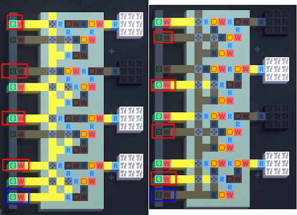
Of course we can also switch between multiple sets of input in a similar way to how we did with the demuxer, though here we get a rapidly shrinking set of data, and lots of inputs


but more generally, it allows us to "program" a sequence of outputs if instead of manually changing the selection pins, we attach this to a clock with a small counter circuit,
Perhaps a program somewhat like
- increment H (program counter)
- read H into G
- Swap G with A
- Copy H to D
- increment H
- read H into G
- Swap G with B
- increment H
- read H into G
- Swap G with C
- E = B - A
- Write E into D
- if E <= 0
- Copy C to H
i'm sure this is highly inefficient but i'll look into optimizing it once i have this working, it's a "safe" implementation.
Of course, then i had to start looking into making a clock/counter.
figured i might have to use some builtin latches for this type of pulse delay partly because i was struggling to build a proper toggle flip-flop, or at least seemingly needing an already functioning clock to get it to work properly (can't build a clock if you need a clock to do so)
i did end up using a DFF, which i showed in part 1, as a source for the clock signal, the builtin latch here sort of also acts as a power button for the computer,  So, from left to right we start with the power button,
then the DFF, looped back into itself to act like a toggle.
then a delay circuit, to make the hysteresis in the DFF look like a constant signal
and then 4 builtin T-flip flops because you can't feasibly get the hysteresis out of the later components, even that first one sometimes just won't start because the hysteresis doesn't stop if you flip the switch on the wrong "phase".
And finally, we have the pulse generator in order to make our clock cycle a pulse, instead of a long signal, since a long signal might screw with the timing-sensitive choreography of the RAM read/write system, which currently runs on that same 2-cycle pulse.
Next up, clearing out some space, and designing our program's inputs, outputs and the different operations i'll need to be able to perform within the CPU


Comments
Post a Comment